Hardware case study / linear view
DSP Rev 3
Rev 3 was nearly assembled but never powered. The complete front and most of the rear were soldered; a small capacitor group and the missing 4.7 µH RT1062 core-buck inductor remained. No Rev 3-specific firmware was written. Its architecture can be explained in detail, but its electrical and software operation must not be presented as demonstrated.
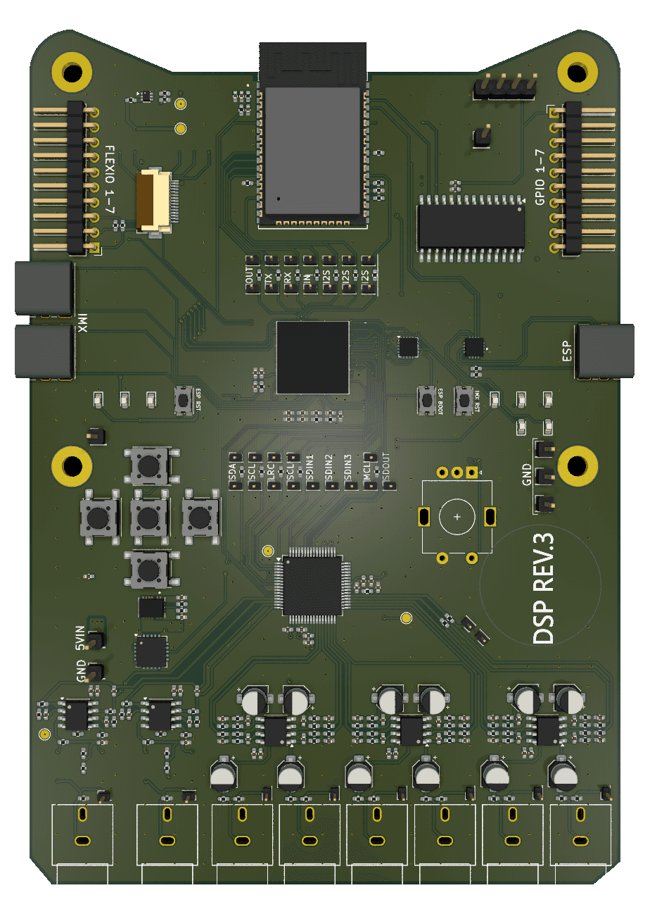
Rotate to inspectLandscape board lab / 640 × 360 minimum
System overview
Core functional architecture
Core functional architecture
RT1062 DSPOnboard DSP processing, codec control, and real-time audio execution.
DSP Rev 3 replaced the removable Teensy 4.1 module with an i.MX RT1062 mounted directly on the PCB. The processor platform includes the MKL02 boot controller, external SPI flash, 24 MHz main reference, 32.768 kHz RTC reference, and the required startup and core-power support network. The processor support circuitry followed PJRC’s Teensy implementation, adapted to Rev 3’s placement and routing.
DSP Rev 3 replaced the removable Teensy 4.1 module with an i.MX RT1062 mounted directly on the PCB. The processor platform includes the MKL02 boot controller, external SPI flash, 24 MHz main reference, 32.768 kHz RTC reference, and the required startup and core-power support network. The processor support circuitry followed PJRC’s Teensy implementation, adapted to Rev 3’s placement and routing.
The RT1062 was designed to handle real-time DSP, codec control, codec-side clocks, ADC and DAC data, and commands from the ESP32.
- intent
Controls CS42526 RESET, I²C configuration, interrupt handling, clocks, and serial audio
- intent
Receives high-level commands and intended Bluetooth-audio data from the ESP32
- confirmed
Uses MKL02 plus external flash for the Teensy-derived boot path
- confirmed
Depends on the complete power/startup sequence before the CPU core can run
- confirmed
Exposes FlexIO-capable signals through the expansion system
The processor platform is implemented in the design, but Rev 3 was never powered. Core-rail startup, bootloader operation, flash loading, USB behavior, codec control, and DSP execution remain unvalidated.
ESP32 InterfaceBluetooth audio, local UI, settings, and interface control.
Rev 3 added an ESP32-WROVER-E interface and connectivity processor so Bluetooth, UI, settings, and browser-based control would not compete with real-time audio processing on the RT1062.
Rev 3 added an ESP32-WROVER-E interface and connectivity processor so Bluetooth, UI, settings, and browser-based control would not compete with real-time audio processing on the RT1062.
The ESP32 and RT1062 were designed as separate processors and clock domains. The intended bridge included an ESP-master I²S audio link, UART-style command traffic, and an additional handshake or interrupt signal. The schematic exposes seven isolated point-to-point connections so the relationship could be probed or separated during bring-up.
- intent
Intended Bluetooth-audio source for the RT1062
- intent
Intended owner of high-level UI state and stored settings
- intent
Sends compact control intent rather than performing the main DSP workload
- confirmed
Connects to the physical controls, screen interface, and GPIO expansion hardware
- confirmed
Uses a dedicated TLV62568-based 3.3 V buck rail
The ESP32 platform and its dedicated 3.3 V supply are implemented in the design, but Bluetooth, UI, browser control, settings, and RT1062 communication were never tested.
CS42526 ConversionTwo-channel ADC and six-channel DAC conversion in one codec.
The CS42526 connects Rev 3’s digital processing to its analog inputs and outputs. It provides two ADC channels for the RCA inputs and three stereo DAC pairs for six output channels, allowing the RT1062 to process incoming analog audio and return independently processed output data through one codec.
The CS42526 provides two ADC channels for the RCA inputs and three stereo DAC pairs for six outputs. It was designed to let the RT1062 process incoming analog audio and send independently processed output data back through one codec.
The RT1062 was designed to control the codec over I²C and act as master for OMCK, LRCLK, SCLK/BCLK, the three DAC data lanes, and the ADC return path. Dedicated 5 V analog and 3.3 V digital/control rails support the codec separately from the processor and op-amp sections.
- confirmed
Two ADC channels
- confirmed
Six DAC channels arranged as three stereo pairs
- confirmed
One I²C control target
- intent
RT1062-master clock and serial-audio relationship
- confirmed
Separate 5 V analog and 3.3 V digital/control rails
- confirmed
Two upstream analog-input interface channels
- confirmed
Six downstream analog-output interface channels
Rev 2 proved the DAC-side architecture. Rev 3 added the ADC path, but its codec communication, initialization, conversion, and audio channels were never tested.
Analog I/OTwo conditioned RCA inputs and six buffered RCA outputs.
The Analog I/O system gives Rev 3 two single-ended RCA inputs and six single-ended RCA outputs around the CS42526. The input side uses active OPA1678 interface stages to convert external single-ended signals into the differential format required by the codec ADCs.
Two OPA1678 stages convert the RCA inputs into the differential signals required by the codec ADCs.
On the output side, three dual OPA1678 packages implement six repeated differential-to-single-ended filter and buffer channels based on the codec reference architecture. The op-amp stages use the quiet 8 V rail, and the buffered outputs leave through six RCA connectors.
- confirmed
Two RCA analog inputs
- confirmed
Two active single-ended-to-differential input channels
- confirmed
Six differential codec DAC outputs
- confirmed
Six active differential-to-single-ended filtered output channels
- confirmed
Six RCA analog outputs
- confirmed
Five total OPA1678 dual-op-amp packages across input and output functions
- confirmed
Quiet 8 V op-amp rail plus codec analog-reference dependencies
Rev 3’s analog I/O was designed around the codec reference architecture, but its input range, output level, impedance, distortion, noise, grounding, protection, and amplifier compatibility were never measured.
Enabling infrastructure
Enabling infrastructure
Power & StartupProtected 9 V input feeding sequenced digital and analog rails.
Rev 3 uses a protected 9 V entry that splits into separate digital and analog power branches. The input passes through a fuse, SMAJ10A transient clamp, and local capacitance before a TPSM863252 generates the 5.4 V intermediate rail and a TPS7A4700 generates the quiet 8 V op-amp rail.
Rev 3 uses a protected 9 V entry that splits into separate digital and analog power branches. The input passes through a fuse, SMAJ10A transient clamp, and local capacitance before a TPSM863252 generates the 5.4 V intermediate rail and a TPS7A4700 generates the quiet 8 V op-amp rail.
The 5.4 V rail feeds dedicated regulators for the CS42526’s 3.3 V digital and 5 V analog supplies, the ESP32’s 3.3 V rail, the RT1062 startup network, and supporting interface hardware. The codec-digital rail also enables the 8 V analog branch, creating an intended sequencing relationship between the conversion and output stages.
- confirmed
Protected 9 V input
- confirmed
TPSM863252 → 5.4 V intermediate rail
- confirmed
TPS7A4700 → 8 V quiet analog/op-amp rail
- confirmed
TLV75733 → 3.3 V codec digital/control rail
- confirmed
TPS7A2050 → 5 V codec analog rail
- confirmed
TLV62568 plus 1 µH L1 → ESP32 3.3 V rail
- confirmed
RT1062 PMIC/startup path → external 3.3 V → internal core buck through missing 4.7 µH L2
RT1062 startup requires PMIC_ON_REQ, the MKL02 boot controller, and the processor’s internal buck through external 4.7 µH L2. L2 was missing from the parts order, so Rev 3 was never powered. No rail, startup, or protection behavior was tested.
Audio & ClockingRT1062-master codec timing with a separate ESP audio link.
Rev 3 has two separate audio links. The RT1062 was designed to master the codec-side clocks and data, sending three DAC lanes and receiving the codec ADC return.
Rev 3 has two separate audio links. The RT1062 was designed to master the codec-side clocks and data, sending three DAC lanes and receiving the codec ADC return.
The RT1062 uses onboard 24 MHz and 32.768 kHz crystals as its operating references. The codec clock and data nets pass through zero-ohm isolation links with probe access on both sides, allowing the processor and converter to be separated or externally observed during bring-up.
- intent
Codec-side master: RT1062
- intent
Codec-side slave: CS42526
- confirmed
Codec clocks: OMCK, LRCLK, SCLK/BCLK
- confirmed
DAC transport: three serial-data lanes for three stereo output pairs
- confirmed
ADC transport: one serial-data return from the codec
- intent
Interprocessor audio: separate intended ESP32-master serial-audio link into RT1062
- intent
Intended sample rate: 48 kHz
- unknown
Runtime format: not recovered or validated
The ESP32 was intended to send Bluetooth audio into the RT1062 through a separate serial-audio link. Rev 3 firmware, clock ratios, framing, synchronization, and audio transport were never tested.
Communication, observability, and support
Communication, observability, and support
USB / BootSeparate programming and recovery paths for both processors.
Rev 3 provides separate programming and recovery paths for both processors. The RT1062 exposes two USB OTG interfaces and uses the MKL02 controller, boot-mode signals, POR control, and a program button to support firmware loading and low-level recovery.
The RT1062 uses two USB OTG interfaces, MKL02 support, boot-mode signals, POR control, and a program button for firmware loading and recovery.
The ESP32 uses a CP2102N USB-to-UART bridge with EN/reset and download-boot controls so it can be programmed without depending on RT1062 firmware.
- confirmed
Two RT1062 USB OTG connector paths
- intent
RT1062 program/boot button and MKL02 recovery relationship
- confirmed
RT1062 POR and boot-mode support
- confirmed
ESP32 CP2102N USB-to-UART bridge
- confirmed
ESP32 EN/reset and download-boot controls
The programming and recovery circuits are present in the design, but USB power, enumeration, bootloader entry, serial programming, and recovery were never tested.
Debug / IsolationIsolation and observability for staged bring-up.
Rev 3 treats observability as a board-level system rather than a collection of accidental probe points. Major rails have labeled test points and indicators, while the codec/RT1062 and ESP32/RT1062 signal groups use zero-ohm isolation links with access on both sides.
Rev 3 includes labeled rail test points, indicators, and zero-ohm isolation links on the codec/RT1062 and ESP32/RT1062 signal groups.
The isolation links were designed to let either processor be separated from the codec, and to make individual clocks and data lines easier to probe during bring-up.
- confirmed
Rail test points and power/status indicators
- confirmed
Codec-side isolation for I²C, OMCK, LRCLK, SCLK, DAC data lanes, and ADC return
- confirmed
RT1062-to-ESP32 isolation and paired access points
- intent
Ability to disconnect a source and inject/observe an external test signal
- confirmed
Boot/status visibility where it serves diagnosis
The debug hardware is built into the design, but it was never used because Rev 3 was not powered.
Expansion / GPIOPhysical interface and expansion hardware.
Rev 3 includes a screen FFC, five pushbuttons, a rotary encoder, an MCP23017 GPIO expander, ESP32 GPIO, and an RT1062 expansion header.
The expansion hardware includes the screen FFC, five pushbuttons, a rotary encoder with push switch, an MCP23017 GPIO expander, ESP-side GPIO, and RT1062 FlexIO-capable signals.
These connections were intended to support the local interface and leave room for later controls or experiments without redesigning the processor core.
- confirmed
Screen FFC and its physical interface signals
- confirmed
Five pushbuttons
- confirmed
Rotary encoder and push switch
- confirmed
MCP23017 GPIO expander
- confirmed
ESP32 auxiliary GPIO/header access
- confirmed
RT1062 FlexIO-capable expansion signals/header
No display, button, encoder, GPIO-expander, header, or auxiliary-I/O behavior was tested.
Deep engineering
Rev 2 → Rev 3: Product-Scale Integration, Unfinished Bring-Up & RedesignRev 2 proved the deliberately simplified audio chain that Rev 1 never completed. Rev 3 preserved that working core, then attempted to surround it with onboard processing, Bluetooth, local controls, analog inputs, expansion, and product-style integration. The board became nearly assembled but never reached first power, making its value architectural rather than functional.
- inference
Rev 3 changed the question from “can the multichannel audio chain work?” to “can that proven chain become a standalone product platform?” Every subsystem needed to earn its cost, interface, startup dependency, firmware burden, and place in the test plan.
Rev 1 exposed coupled unknowns
Rev 1 attempted eight outputs through four stereo codecs before its basic signal chain was validated. Repeated initialization, identical I²C addresses, a mux, two digital-audio groups, distributed master clock, repeated analog interfaces, and difficult firmware were coupled. A critical MCLK route also landed on the Teensy carrier’s neighboring 3.3 V pin rather than the intended clock-capable connection. The route stopped the board, but even a patch would have left control, framing, analog requirements, startup behavior, and firmware unresolved.
Rev 2 narrowed the problem until it could be proven
Rev 2 retained Teensy 4.1, replaced four codecs with one CS42526, used one timing plan, added six buffered outputs, protected the input, and made probing straightforward. It communicated with and configured the codec, generated clocks and serial audio, drove DACs, and produced clean buffered output. Four output channels were exercised individually, two concurrently, and an RCA output fed an external amplifier and speaker.
Rev 3 moved the unknowns upward
Rev 3 integrated RT1062 directly and added ESP32-WROVER-E for Bluetooth, UI, settings, web-style control, and commands. It retained CS42526 for two inputs and six outputs, and added USB paths, screen connection, buttons, rotary encoder, GPIO expansion, independent programming, and deeper isolation. The goal was a standalone device, but bare-processor boot, flash, clocks, reset, USB, ESP software, interprocessor contract, analog inputs, and product controls all became independent risk surfaces.
Where the build stopped
The complete front and most of the rear were soldered. A small capacitor group and RT1062’s 4.7 µH external core-buck inductor remained. The order contained 1 µH ESP-buck inductors, not the RT1062 part. The board was never powered and no Rev 3 firmware was written. The plan was to reuse Rev 2 audio, codec-control, clocking, and DMA work, then extend it for analog input, ESP communication, Bluetooth audio, UI, and DSP. Funding ran out during assembly; attention later shifted to the 600 W Amp + DSP; and the architecture’s shortcomings were already visible.
What Rev 3 demonstrates
Rev 3 demonstrates fabricated, near-complete product-scale integration: component selection, schematic architecture, dense processor support, power distribution, analog I/O, communication paths, and deliberate observability and isolation. It does not demonstrate boot, clocks, communication, conversion, Bluetooth, DSP, display operation, or analog performance.
Current redesign conclusion
A successor would use a purpose-built DSP and newer ESP-class controller; remove screen, buttons, game-style UI, and broad GPIO unless requirements justify them; size the analog regulator to the load; add analog-stage headroom; and begin from downstream amplifier requirements. Complexity must be purchased with a clear requirement, interface contract, startup plan, and proving test.
Evidence to show
- Rev 1, Rev 2, and Rev 3 board comparison
- Coupled complexity → deliberate simplification → product reintegration diagrams
- Rev 2 waveform and RCA → amplifier → speaker flow
- Rev 3 front/back assembly photographs
- Designed / assembled / powered / validated matrix
- Original architecture versus redesign direction
Do not describe Rev 3 as functional, brought up, tested, or failed in operation. Its verified outputs are design files, fabricated board, near-complete assembly, and recoverable engineering decisions.
Bare i.MX RT1062 Integration, Boot & Startup ArchitectureRev 3 replaced the Teensy module with RT1062 and the boot, flash, clock, USB, reset, and power systems the module had hidden. The architecture was based on PJRC’s proven Teensy implementation, but Rev 3 developed its board integration and layout. A missing 4.7 µH inductor prevented first power.
- inference
Moving from a module to a bare processor transfers ownership of complexity to the board designer. A trusted reference reduces conceptual risk, but every support component, sequence, route, footprint, and procurement detail must be correct before one instruction can execute.
From processor user to platform owner
Rev 2 used Teensy 4.1 because it packaged RT1062, bootloader, flash, crystals, power support, USB, and a known software environment. Rev 3 mounted RT1062 directly so DSP lived on one board. In exchange, every system the module supplied had to be recreated.
A reference-derived implementation
The support architecture followed PJRC’s general approach: RT1062, MKL02Z32 boot controller, W25Q16 SPI NOR flash, 24 MHz main crystal, 32.768 kHz RTC crystal, USB, reset and boot controls, external 3.3 V regulation, and RT1062’s internal core buck. Extra decoupling was added in some areas. Placement and routing were original Rev 3 work; this was not a clean-sheet boot architecture.
Startup is a chain
High-input and always-on internal domains wake first. RT1062 then asserts PMIC_ON_REQ to enable external 3.3 V, powering processor I/O, MKL02, and flash. Once stable, MKL02 asserts DCDC_PSWITCH, allowing the internal buck to create approximately 1.15 V core power through the external inductor. Only then can ROM, bootloader, and application code execute. MKL02 also supports reset, boot-mode, debug, data, clock, program-button, and status behavior for recovery and programming.
The missing part that stopped the platform
L2, the required 4.7 µH core-buck inductor, was absent from the DigiKey order. The ordered 1 µH parts are for the ESP buck and are not substitutes. The core-buck path remained incomplete, so the board was left unpowered rather than risking partial startup.
Lesson
Direct integration created learning in BGA support, boot, sequencing, clocks, USB, flash, and dense layout, but much of that work did not directly improve the audio product. Use the most capable platform whose support burden is justified by the application.
Evidence to show
- RT1062 subsystem schematic and processor-area PCB render
- MKL02, flash, crystal, USB, and reset callouts
- Startup-sequence diagram
- Order excerpt and unfinished L2 location
Describe this as a reference-derived RT1062 platform with original board integration and layout. Do not imply that it powered or booted.
Dual-MCU Architecture: Real-Time DSP vs Product ControlRev 3 split real-time audio processing onto RT1062 and Bluetooth, UI, settings, web-style control, and product behavior onto ESP32-WROVER-E. The split had a coherent purpose, but added independent clocks, boot paths, state ownership, streaming transport, commands, and recovery requirements before firmware existed.
- inference
Rev 3 assigned real-time audio, codec control, and DSP to the RT1062, while the ESP32 owned Bluetooth audio, UI, settings, and high-level commands. The processors were connected through defined audio, command, and handshake links.
Intended roles
RT1062 was intended to configure CS42526, generate codec clocks, move ADC/DAC samples, execute DSP, and apply gain, routing, and filter changes. ESP32 was intended to receive Bluetooth audio and handle screen, controls, settings, web-style interface, spare GPIO, and high-level commands. The objective was to protect real-time audio from UI and connectivity work.
Streaming versus control
I²S was planned for Bluetooth audio, with ESP32 remembered as master. UART TX/RX provided commands for volume, filters, routing, and settings. An additional GPIO was intended for ready/busy, interrupt, handshake, or synchronization, but its exact role was never finalized. The seven physical point-to-point links can be isolated and probed.
Independent domains and defined links
The ESP32 and RT1062 use separate clocks and boot paths. The interprocessor architecture defined audio transport, command traffic, and a handshake link between them. Rev 3 never reached firmware integration or hardware validation of those connections.
Lesson
The processor split gave real-time audio and product-interface work clear owners. A next revision should keep that separation while limiting UI, expansion, and extra controls to features supported by the product requirements.
Evidence to show
- RT1062/ESP responsibility matrix
- Physical-link and separate-clock/boot-domain diagrams
- UI, GPIO expander, and expansion callouts
- Original dual-MCU direction versus DSP + modern ESP direction
Rev 3 defined the dual-MCU architecture, but Bluetooth audio, interprocessor communication, settings, UI, and web control were never implemented or tested.
Audio, Clock & Data ArchitectureRev 3 retained the codec-side timing relationship that worked in Rev 2, then added analog input through CS42526 ADCs and Bluetooth audio through ESP32. RT1062 remained master of the codec domain; ESP32 added a second independent clock domain without a completed buffering or synchronization strategy.
- inference
Preserving the known RT1062-to-CS42526 core was Rev 3’s strongest audio decision. Its largest unresolved audio problem was transferring a continuous stream from an independently clocked ESP32 into RT1062 without defined drift, buffering, flow control, or recovery behavior.
The earlier clock lesson
Rev 1 attempted to distribute 12.288 MHz MCLK while Teensy generated the remaining audio timing. The intended MCLK branch landed on a neighboring 3.3 V carrier pin, and the board never achieved working codec audio. The broader failure was that timing had not been treated as one complete architecture.
Rev 2 corrected this with one master: the RT1062 within Teensy generated MCLK, BCLK, LRCLK, and serial audio for CS42526. Recovered firmware shows a 48 kHz system with 12.288 MHz MCLK, 3.072 MHz BCLK, 24-bit samples in 32-bit stereo slots, and multiple TX lanes feeding DAC pairs. That configuration produced working analog output.
Rev 3 froze the proven codec-side relationship
The bare RT1062 was intended to remain codec master. The schematic routes OMCK, shared LRCLK, shared SCLK/BCLK, three DAC serial-data lanes, one ADC serial-data return, plus I²C, RESET, and interrupt relationships. Zero-ohm links and probe access allow individual signals to be disconnected, observed, or externally driven.
Exact Rev 3 frequencies and framing were never implemented. A 48 kHz system was intended, with Rev 2 firmware serving as a planned baseline rather than a Rev 3 measurement.
Expanded entry paths and two clock domains
Two RCA inputs would pass through active stages to CS42526 ADCs, return digitally to RT1062, receive DSP, and leave through six DAC/output channels. ESP32 would receive Bluetooth audio and transfer it to RT1062 over separate I²S. A direct digital entry was conceptually possible through RT1062, but no dedicated external digital-audio connector is recovered in the root schematic.
The RT1062 owned codec timing, while the ESP32 was designed to send Bluetooth audio through its own serial-audio link. The processors used separate clock domains and defined audio, command, and handshake connections, but Rev 3 never reached firmware integration or hardware validation of that bridge.
Lesson
Reuse proven timing cores, but treat every new clock-domain boundary as a new architecture with explicit buffering, ownership, startup, and failure behavior.
Evidence to show
- Rev 1 incorrect-MCLK connection versus Rev 2 single-master domain
- Rev 2 recovered clock values and waveform
- RT1062-to-CS42526 map and audio-entry path diagram
- ESP32/RT1062 independent-clock-domain diagram
- Isolation links and planned firmware-reuse map
Rev 2 clock values were the baseline for Rev 3’s codec-side design. Rev 3’s clocking and ESP32-to-RT1062 audio bridge were defined but never implemented or tested on hardware.
Power Architecture, Sequencing & Subsystem IndependenceRev 3 used protected 9 V entry, 5.4 V switching backbone, quiet 8 V analog branch, local codec and ESP regulators, and RT1062’s multi-stage startup sequence. Removable links and injection points were intended to permit independent subsystem power and test.
- inference
The power tree was designed both to operate a mixed-signal system and to diagnose it. Its most mature decision was not a particular regulator, but the attempt to make rails and loads separable and independently testable. No part of the complete system was proven because first power never occurred.
Protected entry and rail split
Approximately 9 V enters through a fuse, SMAJ10A TVS clamp, and ceramic/bulk capacitance. The recovered root schematic does not show confirmed reverse-polarity protection, so Rev 3 must not inherit that claim from Rev 2. TPSM863252 creates the 5.4 V intermediate rail; TPS7A4700 is fed directly from protected input and creates 8 V for OPA1678 analog stages.
Local load-class rails
5.4 V feeds TLV75733 codec-digital 3.3 V, TPS7A2050 codec-analog 5 V and input biasing, and TLV62568 plus 1 µH L1 for ESP32, MCP23017, CP2102N, and ESP support. The codec-digital 3.3 V net also controls 8V_EN, expressing the intended relationship that op-amp rail should not enable until codec digital rail is present. The processor startup network and screen/interface branch also derive from the system infrastructure.
Processor sequencing
Beyond the rail tree, always-on RT1062 domains wake, PMIC_ON_REQ enables external 3.3 V, MKL02 and flash become powered, then MKL02 asserts DCDC_PSWITCH so the internal buck can create approximately 1.15 V through 4.7 µH L2. If external 3.3 V, MKL02 state, switch, inductor, or core network is wrong, CPU cannot reach ROM execution.
Debug boundaries
The design intended codec and ESP to remain isolatable if RT1062 failed; codec rails could be disconnected and lab-supplied; clock links could be opened and externally driven; and ESP/RT1062 communication links could be isolated. This extends Rev 2’s links and selective access into an explicit board architecture of isolation, injection, and observability.
Missing L2 and redesign lesson
The 4.7 µH L2 was not ordered; 1 µH ESP parts are not substitutes. The board was not powered, so no rail voltage, ripple, timing, protection, injection, or thermal behavior was measured. A redesign should size analog regulation to actual load while providing useful voltage headroom. A prototype power tree must define both how a system runs and how each subsystem can be proven without trusting the rest.
Evidence to show
- Protected-input and full rail map
- Startup chain diagram
- Rail test points, indicators, links, and injection boundaries
- Missing-L2 order comparison and staged first-power checklist
Describe the tree and sequencing as implemented design. Do not claim measured rail behavior, isolation success, protection performance, or thermal margin.
Analog I/O Design & Missing External RequirementsRev 3 expanded Rev 2’s output concept into two active analog inputs and six active analog outputs around CS42526. The circuits were materially more complete than Rev 1, but downstream electrical requirements—especially amplifier compatibility—were not defined before the topology was selected.
- inference
Copying a codec reference circuit is not the same as defining a product interface. Source, load, level, ground relationship, protection environment, and performance targets must drive the circuit.
Progression across revisions
Rev 1 wanted one stereo input and eight outputs without engineering the interfaces around real sources or loads. Rev 2 corrected output: CS42526 produced six differential DAC channels and repeated OPA1678 stages converted, filtered, and buffered them into RCA outputs. It produced measured sine output and fed an external amplifier and speaker. Rev 3 retained that output architecture and added the input direction.
Two active inputs and six active outputs
Two RCA inputs were intended to enter CS42526 ADCs through OPA1678 stages that create the differential pair required by the converter and present expected source conditions. The topology was based on the codec reference design, not a formal product requirement.
Three stereo DAC pairs create six differential outputs. Three dual OPA1678 packages implement six differential-to-single-ended filtering/buffer channels from a quiet 8 V rail to six RCA connectors. The filters were intended to reduce out-of-band converter noise and present a practical signal to external amplification.
Physical capacity is not a specification
Rev 3 had no locked consumer, professional, or automotive target for headroom, Vrms, source/load impedance, cable length, DC fault, ESD, short protection, noise, distortion, matching, or amplifier compatibility. External grounding through RCA shields, supplies, and downstream amplifier was not fully defined. “Two inputs and six outputs” describes channel architecture—not qualified interface performance.
Lesson
A redesign should begin with downstream amplifier impedance, required level, cable/ground arrangement, noise target, faults, and available supply headroom. More useful op-amp headroom, a load-appropriate regulator, and explicit ground-loop requirements should follow. First define the external interface, then choose and calculate the converter support circuit.
Evidence to show
- Rev 1/2/3 analog comparison and two-input/six-output map
- Single-ended-to-differential and differential-to-single-ended diagrams
- OPA1678/8 V callouts
- RCA-to-amplifier requirements table and future measurement plan
Do not call Rev 3 automotive-compatible, amplifier-qualified, or formally line-level compliant. No Rev 3 analog path was powered or measured.
PCB Layout, Grounding, Signal Integrity & DebugabilityRev 3 used four layers with fast routing concentrated on top over solid ground, slower/escape routing on bottom, internal power/mixed routing, analog separation, pours, stitching, fencing, and unusually deep subsystem isolation. Local plane slots and an unpowered board prevent claims that these choices were validated.
- inference
The revision progressed from routing traces to designing signal paths and test boundaries. Ground copper and vias do not guarantee continuous return paths, and a design remains unproven until the fabricated board is measured.
Preferred high-speed environment
The stack was L1 top/components/primary fast routes, L2 main solid ground, L3 power/mixed routing, and L4 bottom/components/slower and escape routing. L1 and L4 were not treated as equivalent high-speed layers. Fast routes were intentionally kept on L1 where possible so they referenced L2 directly; bottom was mainly slower traffic and unavoidable escape/cross-under routing.
Signal priority and analog separation
Fast traces were kept away from unrelated circuitry and crossings were avoided where they lacked solid ground separation. When crossings were necessary, their risk was judged by signal speed rather than arbitrary geometry matching. Analog input/output circuitry was grouped near the lower board, and fast digital traffic was kept out so analog ground did not become the main return path for processor traffic.
Stitching, fencing, and local plane damage
Pours, via stitching, and fencing were intended to improve ground continuity, connect local pours, contain return current, and create a coherent reference. This was a methodological step forward. Execution was not perfect: clearances and antipads around dense RT1062 routing created local slots and narrow ground paths. Dense stitching can undermine the plane it is meant to help; density, antipad geometry, escape routing, and continuity must be reviewed as one electromagnetic structure.
Debugability as physical architecture
Rev 3 made RT1062-to-codec clock, data, and control links disconnectable and accessible on both sides; the ESP links received similar treatment. Major rails could be separated and lab-supplied. The intent was that a dead RT1062 would not prevent codec/ESP study, and that external known clocks could be injected into an isolated codec side. Everything important should be measurable, isolatable, injectable, and falsifiable one system at a time.
What it proves
Schematic and PCB architecture show improved routing discipline, grounding intent, analog separation, and debug planning. Because the board was never powered, they do not prove ringing, crosstalk, jitter, noise, return-current behavior, EMI, or analog performance.
Evidence to show
- Four-layer stack and critical-route maps
- Analog-separation and pour/stitching overlays
- RT1062 via-antipad/ground-slot examples
- Codec/ESP isolation diagrams and revision-to-revision debug comparison
Do not claim impedance control, EMI reduction, or signal-integrity testing. Describe design intent, observable geometry, local plane damage, and unperformed measurements separately.