Hardware case study / linear view
DSP Rev 2
Functional validation prototype: codec communication, working digital audio, measurable analog output, and RCA playback through an external amplifier and speaker.
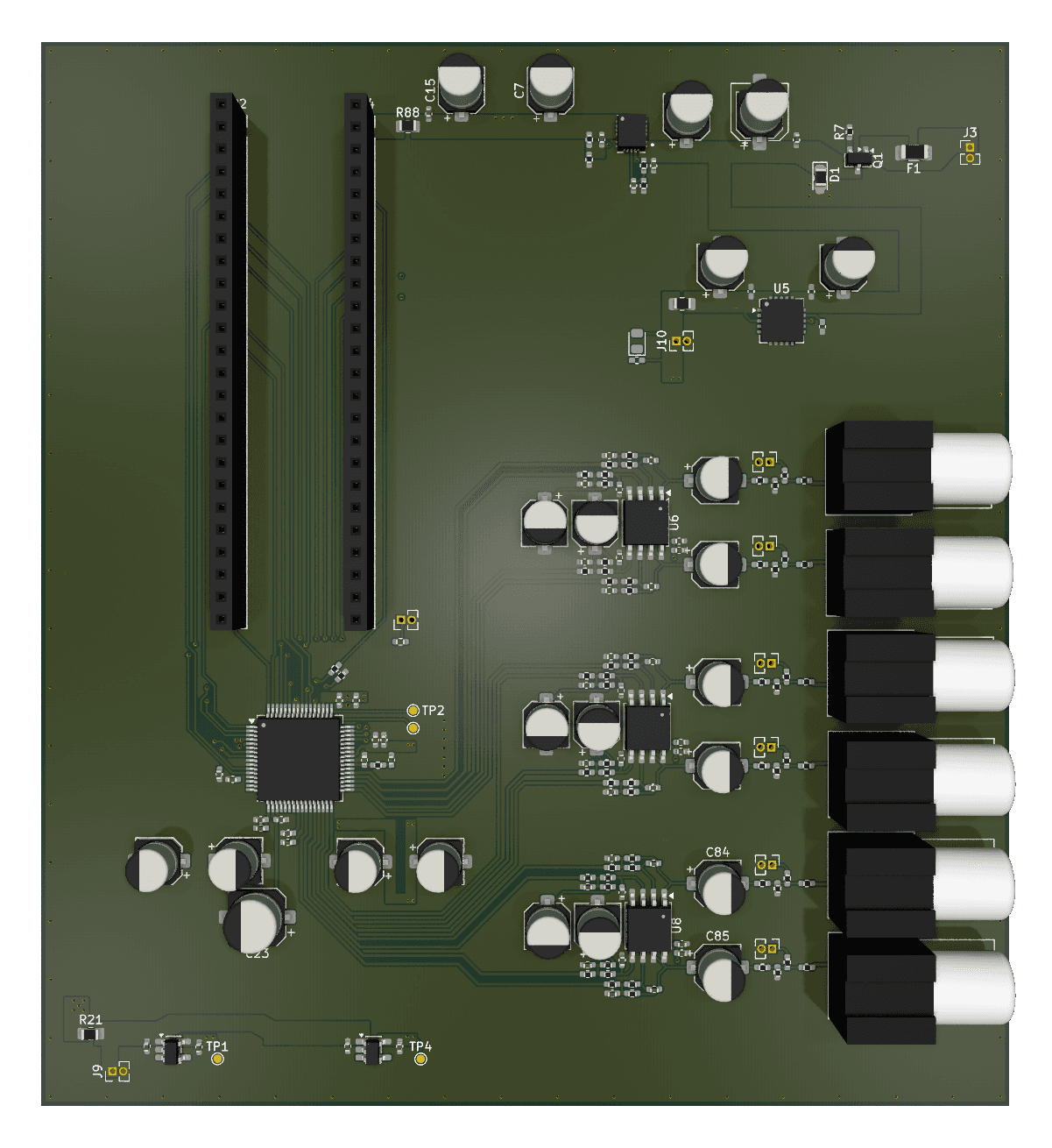
Rotate to inspectLandscape board lab / 640 × 360 minimum
System overview
Core signal system
The controller, conversion core, and six-channel analog output path.
Teensy HostAudio-clock generation, codec control, and DSP execution.
Rev 2 retained the Teensy 4.1 because it combined high processing performance, small physical size, low cost, extensive support, and audio-capable SAI hardware. The Teensy became the active center of the system: it controlled codec reset, communicated over I²C, programmed and verified codec registers, generated the audio clocks, transmitted sample data, and produced the test signal used to validate the DAC and analog output stage. The recovered source is slightly behind the final bench build and predates its basic volume-control feature.
- confirmed
The Teensy booted, controlled codec RESET, identified the CS42526 over I²C, and programmed and read back its registers.
- confirmed
The firmware generated 12.288 MHz MCLK, 3.072 MHz BCLK, 48 kHz LRCLK, and transmitted serial audio through a custom SAI1/DMA path.
- confirmed
The Teensy-generated sine signal produced measurable analog output through the codec and output stage.
- unknown
Complete production DSP firmware, final USB audio behavior, full six-channel processing, and product-level control software were not validated.
Validated for MCU operation, I²C communication, register programming/readback, audio-clock generation, serial-audio transmission, sine generation, and analog output. Rev 2 remained a validation platform rather than a complete automotive DSP application.
CS42526 CodecOne six-output conversion core replacing Rev 1's four-codec bank.
The CS42526 is the defining architectural change of DSP Rev 2. Rev 1 used four repeated stereo codecs and required control isolation, distributed clocks, repeated initialization, and more complicated routing. Rev 2 replaced that structure with one multichannel converter providing three stereo DAC pairs. The codec was selected for six-output capacity, 24-bit support, 48 kHz operation, manageable configuration, low cost, and a pin arrangement compatible with the Teensy's serial-audio lanes. Its ADC and receiver capabilities were deliberately outside the tested Rev 2 path. Firmware identified the device, wrote and read back its configuration, released the DACs from power-down and mute, and produced working analog output.
- confirmed
The codec presented one I²C target, one shared timing domain, three stereo DAC pairs, and six downstream OPA1678 output channels.
- confirmed
I²C acknowledgement, chip identification, register writes/readback, and DAC operation were demonstrated.
- measured
Four distinct analog channels were exercised across separate tests and two channels were operated concurrently.
- unknown
ADC operation, four or six simultaneous outputs, receiver features, and formal codec performance were not validated.
The conversion architecture worked in the tested configuration. The part's discontinued or constrained lifecycle remained a sourcing lesson, and physical six-channel capacity must not be presented as six-channel simultaneous validation.
Analog OutputsSix buffered line outputs from three differential DAC pairs.
Rev 2 added a real analog-output stage instead of assuming raw codec pins could be exposed directly. Each CS42526 DAC channel enters a repeated filter and differential-to-single-ended circuit based closely on the codec reference design. Three dual-channel OPA1678 sections support six intended outputs from the quiet 8 V TPS7A4700 rail. RCA connectors let the board act as a line-level source for downstream amplification. Bench validation measured the output on an oscilloscope and connected one RCA path to an external amplifier that powered a speaker.
- confirmed
The physical board contains six buffered RCA output paths from three differential DAC pairs.
- measured
Clean analog sine output, four individually exercised channels, and two concurrent channels were demonstrated.
- confirmed
The confirmed playback chain was Rev 2 RCA output to an external amplifier to a speaker; the board did not directly drive the speaker.
- unknown
Six-channel concurrent output, frequency response, THD+N, SNR, crosstalk, channel matching, output impedance, and automotive protection were not validated.
The analog implementation worked as a validation output, but the external interface was not derived from a formal automotive or line-output requirements document.
Enabling infrastructure
Protected multi-rail power and one coherent digital-audio clock domain.
Power & ProtectionProtected 9 V input feeding the analog, Teensy, and codec rails.
Rev 2 replaced Rev 1's trusted-bench-power assumption with a protected, multi-rail tree. Approximately 9 V enters through a two-pin connector, a confirmed 1.25 A fuse, AO3401A P-channel reverse-polarity stage, SMAJ10A TVS clamp, and bulk filtering. A TPS7A4700 generates the quiet 8 V OPA1678 rail. A TPSM863252 generates approximately 5.2 V for the Teensy branch and downstream TPS7A2050 5 V and TLV75733 3.3 V codec rails. Removable links isolate major regulator outputs and loads during troubleshooting.
- confirmed
The protection chain uses a 1.25 A fuse, AO3401A reverse-polarity MOSFET, SMAJ10A TVS diode, and input capacitance.
- confirmed
The rail tree produced 8 V analog, approximately 5.2 V main, 5 V codec, and 3.3 V codec branches.
- measured
Board power-up, rail voltages, total current, rough thermal behavior, and downstream digital and analog operation were observed.
- unknown
Ripple, load transients, thermal margin, efficiency, inrush, fault energy, and automotive electrical transients were not characterized.
Protected bench-prototype power was validated functionally. The approximately 5.2 V buck target compensated for observed sag and is documented as a prototype workaround, not a sound production design method.
Audio & ClockingOne Teensy-master timing domain feeding multiple stereo data lanes.
Rev 2 corrected the timing relationship that stopped Rev 1. The Teensy became external master for the complete tested interface: 12.288 MHz MCLK, 3.072 MHz BCLK, and 48 kHz LRCLK, with 24-bit samples carried in two 32-bit I²S slots. Shared clocks and multiple physical stereo data lanes feed the CS42526 DAC pairs. Critical routes were kept short, layer changes were minimized, broad ground reference was preserved where practical, and approximately 10 Ω source damping resistors were added without imposing Rev 1's arbitrary ±2 mm matching target.
- confirmed
The Teensy operated as master and the CS42526 as slave in one synchronized SAI/I²S clock domain.
- confirmed
The recovered firmware establishes 48 kHz, 12.288 MHz MCLK, 3.072 MHz BCLK, two 32-bit slots, and 24-bit audio payloads.
- measured
Clocks and serial audio operated sufficiently to produce repeatable DAC and analog output in the tested configuration.
- unknown
Formal jitter, edge-rate margin, timing margin across voltage and temperature, and simultaneous six-channel data operation were not validated.
The correct description is one synchronized SAI/I²S clock domain with multiple stereo data lanes—not two unrelated I²S buses.
Communication and debug
The isolation, probing, and repair access used during successful bring-up.
Debug AccessAn oversized validation board designed for isolation, probing, and repair.
The approximately 128 mm × 114 mm board was intentionally larger than necessary. Rev 2 traded density for clear routing, physical access, and easier fault isolation. Power rails and analog outputs received deliberate access, while clocks, data, and control could often be probed at accessible Teensy pins. Zero-ohm links created useful power boundaries without adding stubs to every signal. Small 1.27 mm headers were weak field connectors but held oscilloscope hooks well; the two-pin power connector remained awkward and required soldered wires for reliable bench clips.
- confirmed
The board used large sparse placement, accessible Teensy pins, rail and output test access, zero-ohm isolation, repeated analog sections, and broad four-layer reference areas.
- confirmed
These features supported power checks, codec bring-up, differential measurement, corrupted and clean waveform capture, and the amplifier/speaker demonstration.
- unknown
The board did not expose every possible injection or current-measurement boundary, and not every subsystem could be powered independently.
The debug architecture served the validation goal. It should not be presented as complete subsystem isolation or as proof that every exposed pin was a purpose-built test point.
Deep engineering
Rev 1 → Rev 2: Architectural SimplificationRev 2 reduced the system to one controller, one codec, one coherent clock domain, and one measurable output chain so the fundamentals could be proven.
- confirmed
Rev 2 retained one Teensy 4.1, replaced four codecs with one CS42526, and prioritized access over density.
- measured
The simplified chain reached codec control, audio conversion, four individually exercised channels, two concurrent channels, and external-amplifier playback.
The problem inherited from Rev 1
Rev 1 combined four codecs, repeated control, multiple audio paths, distributed clocking, and unfinished firmware before producing working audio.
Redefining success
Rev 2 narrowed success to protected power, communication with one codec, reliable configuration, coherent clock and serial audio, a measurable analog sine wave, and a real amplifier connection if possible. Analog inputs, complete filters, presets, product packaging, and polished control software were intentionally outside that question.
The simplification decisions
The Teensy stayed for its performance, SAI hardware, support, and DSP headroom. One CS42526 removed repeated addresses, the I²C mux, repeated initialization, and distributed codec clocks. A deliberately large four-layer board separated power, codec, analog, and measurement regions while using practical routing constraints rather than cosmetic matching.
What the simpler architecture proved
Rev 2 proved the complete path from reset and codec configuration through DAC conversion, RCA output, and amplifier playback. Four outputs were exercised separately and two concurrently.
Rev 2 answered its core question: can a simpler architecture deliver verified audio?
Power Architecture, Protection & IsolationRev 2 added protected input power, separate branches, and removable boundaries, but the 5.2 V buck setting concealed an unresolved voltage drop.
- confirmed
The input uses a 1.25 A fuse, AO3401A reverse-polarity MOSFET, SMAJ10A TVS clamp, and input capacitance.
- measured
Approximately 166–168 mA total current appeared in both working and non-working output states, so current alone did not diagnose audio state.
Power requirements and input protection
The board had three different loads: Teensy and the main digital branch, CS42526 5 V and 3.3 V rails, and OPA1678 analog stages. Approximately 9 V enters through the small bench connector, then passes the confirmed Bel C1F 1.25 A fuse, AO3401A P-channel reverse-polarity stage, SMAJ10A transient clamp, and bulk and local capacitance.
The connector was mechanically weak for bench use, so wires were soldered into the area to create a dependable alligator-clip connection.
Split regulation architecture
A reused TPS7A4700 creates the quiet 8 V rail for the analog output stages. A TPSM863252 generates approximately 5.2 V for the Teensy and downstream TPS7A2050 5 V and TLV75733 3.3 V codec regulators. This keeps the higher-current conversion upstream and gives the codec local LDO supplies.
The 5.2 V compensation mistake
The buck was set above 5 V to offset observed sag. That enabled bring-up, but it concealed the cause of the voltage drop rather than solving it.
Isolation, capacitance, and evidence
Removable links helped check regulators before reconnecting loads. Rail voltage, total current, and rough thermal behavior were observed; ripple, transients, efficiency, sequencing, and thermal margin were not characterized.
The power system supported protected bench testing; automotive transient qualification remains untested.
Digital Audio & Clock ArchitectureOne Teensy-master SAI domain fixed Rev 1's clock relationship, while a 2.66 ms waveform pattern exposed a separate DMA-buffering fault.
- confirmed
Recovered firmware directly configures the audio PLL, SAI1, pin mux, FIFO, and DMA for standard I²S operation.
- inference
The approximately 2.66 ms corruption period aligned with the 128-frame DMA half-buffer interval and pointed to the firmware service boundary.
One coherent audio-interface plan
The codec needed six-output capacity at 48 kHz with 24-bit samples. Rev 2 avoided one large TDM frame and instead used shared clocks with multiple physical serial-data lanes, preserving two-slot stereo framing inside one synchronized domain.
The Teensy generated 12.288 MHz MCLK, 3.072 MHz BCLK, and 48 kHz LRCLK. Each frame contains two 32-bit I²S slots with 24-bit payloads. The Teensy is master and the CS42526 is slave. Recovered source confirms standard I²S framing.
Multiple lanes and routing strategy
Multiple SAI transmit lines feed the codec's three stereo DAC inputs and can duplicate a stereo pair across lanes. This is one synchronized SAI/I²S domain with multiple stereo data lanes—not two independent I²S buses.
Routing kept clocks and audio paths short, with few branches and layer changes plus roughly 10 Ω source damping. The working board still had avoidable plane damage and reference transitions.
DMA timing as a debug signature
A 128-frame DMA half-buffer repeats every 2.667 ms at 48 kHz. Bursts observed near 2.66 ms pointed to the buffer-service boundary, not the analog filter.
The buffering fault was fixed, but its exact mechanism was not recovered.
A coherent timing plan mattered more than trace optimization. The buffering fix is confirmed; its exact failure mechanism is not.
CS42526 Firmware, Reset & InitializationDeterministic reset, verified register programming, muting, health checks, and recovery made the codec functional; one USB-linked startup quirk remained unresolved.
- confirmed
The fabricated board omitted the intended RESET pulldown and was repaired with an external resistor or jumper.
- confirmed
Firmware verified chip identity and read back each programmed configuration register.
- unknown
The exact mechanism behind laptop/USB-connected startup and reflash behavior was not recovered.
Reset hardware and startup state
The fabricated board omitted the RESET pulldown, so RESET floated until the Teensy drove it. An external resistor/jumper repair made startup deterministic.
Verified startup sequence
Firmware holds RESET, verifies I²C and chip ID, programs and reads back the configuration, then unmutes audio. A health failure mutes outputs, recovers I²C, reasserts RESET, and retries.
The table configures 48 kHz single-speed operation, standard I²S, codec slave mode, ADC power-down, all three DAC pairs, initial volumes, setup mute, and final analog unmute.
Recovered firmware and USB-linked behavior
Recovered firmware predates the final bench-build volume control.
Output could become unreliable after laptop connection or reflash; a full disconnect and restart restored operation. The root cause was not recovered.
The reset workaround is confirmed; the laptop/USB startup cause remains unknown.
Differential Analog Output DesignSix repeated OPA1678 channels proved a real RCA-to-amplifier path while exposing the difference between copying a reference circuit and defining an interface.
- confirmed
Analog inputs were deliberately omitted; Rev 2 focused on proving digital samples could become usable outputs.
- measured
Four outputs were exercised separately, two concurrently, and one RCA path fed an external amplifier and speaker.
Differential-to-single-ended conversion
The CS42526 provides three stereo differential DAC pairs. Each channel feeds a repeated active filter and differential-to-single-ended stage based closely on the codec reference circuit. Three dual-channel OPA1678 sections provide six outputs from the quiet 8 V rail and present them through RCA connectors.
Measurement topology mattered
The analog stage initially looked inactive because the differential signal was interpreted against an inappropriate or floating reference. Two probes across the differential nodes revealed the actual sine wave. The probe connection was part of the measurement system.
Real playback and validation boundary
The verified path was RCA output into an external amplifier, then a speaker. Four channels were exercised separately and two concurrently.
No formal electrical or environmental characterization of the output interface was completed.
The board did not directly drive a speaker, and concurrent six-channel output was not demonstrated.
Prototype Layout & DebugabilityThe oversized board simplified routing, isolation, probing, and repair while exposing where visually neat via rows can damage a reference plane.
- confirmed
The approximately 128 mm × 114 mm board was intentionally oversized for access and fault isolation.
- inference
Clustered ground-via antipads created local slots or necks in reference copper even though stitching intent was sound.
Layout optimized for learning
The board kept systems separated, routing legible, layer transitions limited, probes and clips accessible, jumper repair possible, and repeated analog sections easy to compare. Density, enclosure fit, and manufacturing cost were not primary constraints.
The board used a shared ground system: ground fill on Layers 1 and 4, a primary ground plane on Layer 2, and power distribution with substantial ground on Layer 3.
Selective access and isolation
Rev 2 exposed main rails, analog outputs, isolation links, accessible Teensy clock/data/control pins, and small hook-friendly headers instead of putting long test stubs on every net. Disconnectable links could change the circuit boundary, making them more useful than observation-only pads.
Plane and connector lessons
Ground stitching and perimeter vias were intended to improve continuity, but visually neat rows of antipads removed copper and locally narrowed the reference plane. More ground vias are not automatically better when their clearances damage the plane they should support.
The two-pin power connector was awkward enough to require soldered wires for clips. RCA outputs matched the actual amplifier test better. Connector selection should follow the test and use environment, not schematic convenience.
Rev 2's size made routing, probing, isolation, and repair easier. The next layout should retain that access while improving plane continuity and connector choice.
Functional Bring-Up, Validation & Why Rev 3Rev 2 closed the audio chain, then moved on once its validation objective was achieved.
- confirmed
Rev 2 reached protected power, deterministic RESET after repair, codec communication, verified register programming, synchronized serial audio, DAC conversion, buffered RCA output, and speaker playback through an amplifier.
- measured
Four distinct outputs were exercised across separate tests and two were operated concurrently.
- unknown
Six or four simultaneous outputs, full DSP, final USB/music behavior, formal analog performance, and automotive robustness were not validated.
Reconstructed bring-up sequence
Bring-up progressed from protected power and controller operation through RESET repair, codec configuration, validated audio, buffer debugging, channel tests, and amplifier playback.
Confirmed success and remaining startup limit
Laptop connection or reflash could leave output unreliable; a full disconnect and restart restored operation. The root cause remains unknown.
Why two channels were enough
Four channels were exercised separately and two concurrently. Once the full audio path worked, further simultaneous-channel testing had less value than the next integration question.
Why Rev 3 became more ambitious
Rev 3 was intended to turn the proven chain into a far more integrated standalone platform: onboard i.MX RT1062, an ESP-class interface controller, no removable Teensy module, and more product-oriented power and interfaces. It was a deliberately high-risk experiment rather than a conservative Rev 2 cleanup.
Rev 1 exposed an over-complex architecture. Rev 2 proved a simpler audio chain. Rev 3 used that proof as the basis for a more integrated experiment.
Rev 2 implemented six outputs, exercised four individually, and demonstrated two concurrently. It succeeded by proving the audio chain, not by becoming a finished product.