Hardware case study / linear view
DSP Rev 1
Electrical bring-up succeeded, but the digital-audio and analog signal chain was never functionally validated.
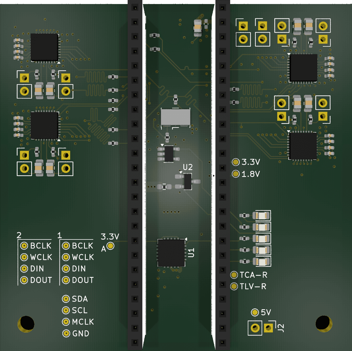
Rotate to inspectLandscape board lab / 640 × 360 minimum
System overview
Core signal system
The processing, conversion, and analog paths the board existed to provide.
Teensy / MCUUSB audio processing, multichannel distribution, and codec control.
The Teensy 4.1 was intended to receive a stereo USB audio stream, perform fixed DSP including routing, mixing, volume, delay, EQ, and crossover processing, and distribute the resulting channels across two I²S/TDM buses. It also controlled codec configuration through an I²C mux and drove two general-purpose status LEDs.
- intent
Planned processing included routing, mixing, level adjustment, delay, basic EQ, and crossover filtering across eight logical outputs.
- intent
No user-facing configuration application, preset system, or runtime tuning interface was planned.
- confirmed
The Teensy powered, could be programmed, and ran basic blink firmware.
- unknown
Final routing, filters, channel numbering, codec setup, and the exact external-MCLK firmware configuration were never completed or verified.
The Teensy powered and accepted firmware uploads, but USB audio streaming, codec communication, DSP processing, and the complete audio path were never functionally validated.
Codec BankFour repeated stereo conversion sections linking the digital buses to the analog connectors.
Four stereo codecs provided the planned capacity for eight analog outputs. The upper-right codec also provided the board's only planned stereo analog input. Two codecs shared each I²S/TDM bus, while an I²C mux allowed the Teensy to individually address four codecs that otherwise shared the same control address.
- intent
The target system was intended to operate around a 48 kHz sample rate with a 12.288 MHz codec master clock.
- intent
The upper-right device was assigned stereo ADC and DAC duties; the remaining three devices were intended for DAC output only.
- inference
The visible package marking probably identifies the codec as a TI TLV320AIC3104, but the surviving part has not been checked closely enough to confirm it.
- measured
With the Teensy removed, approximately 12.288 MHz was observed at all four codec areas.
- unknown
Codec-local rails, I²C acknowledgement, register initialization, TDM operation, ADC operation, DAC operation, and analog performance were not validated.
The codec hardware was assembled and, with the Teensy removed, MCLK reached all four codec areas, but codec initialization, I²C communication, TDM operation, ADC operation, and DAC operation were never validated.
Analog I/OOne planned stereo input and four planned stereo output pairs.
Rev 1 included one planned stereo input and four stereo output pairs, giving the board two analog input channels and eight analog output channels. Passive coupling and filtering networks connected these interfaces to the codec bank.
- intent
The outputs were loosely imagined for oscilloscope measurement or connection to an external amplifier.
- confirmed
Input, output, and associated passive components were physically assembled.
- unknown
Levels, impedance, cable behavior, connector pin order, ground returns, buffering, protection, and the external load were not formally defined or validated.
Input level, output level, source/load impedance, grounding, cable requirements, buffering, protection, and connector behavior were not fully specified, and the analog signal paths were never functionally validated.
Enabling infrastructure
Power, clocking, startup, and protection needed to support the signal system.
Power TreeConverts the external 5 V input into the board's main 3.3 V, 1.8 V, and clock-section rails.
External 5 V entered through a two-pin header. Raw 5 V supplied the Teensy while separate regulator sections generated the board's 3.3 V and 1.8 V rails, including a dedicated 3.3 V regulator for the clock section. Three rail LEDs and accessible power test points supported basic bring-up.
- confirmed
Board-level 3.3 V and 1.8 V were measured at test points, and the three rail LEDs operated.
- unknown
Per-codec rails, ripple, transient response, efficiency, junction temperature, and thermal margin were not measured.
Board-level 3.3 V and 1.8 V rails were successfully measured, but per-device voltages, ripple, transient behavior, and thermal performance were not characterized.
Clock TreeDistributes a dedicated 12.288 MHz master clock toward four codecs and the intended Teensy clock connection.
One dedicated 12.288 MHz oscillator was intended to supply MCLK to all four codecs and reach a Teensy clock-capable or MCLK-related connection. The Teensy was intended to generate BCLK and WCLK/LRCLK while the codecs operated as slaves. A source damping resistor was included for later tuning.
- confirmed
The designed Teensy trace connected to the neighboring 3.3 V pin instead of its intended clock-capable connection.
- measured
With the Teensy removed, approximately 12.288 MHz was observed at the oscillator, MCLK test point, and all four codec areas.
- measured
The measurements showed overshoot, undershoot, post-edge ringing, and different waveform shapes at different points on the board.
- unknown
The original Teensy clock configuration, the waveform with the Teensy installed, any electrical stress at the 3.3 V pin, and the cause of codec non-operation were not established.
The clock network distributed a signal on the unpopulated-carrier test, but the Teensy destination error ended confidence in the as-built architecture.
Reset & StartupThe assumed sequence from rail rise and clock start through controller boot and codec initialization.
Rev 1 had no coordinated startup sequence. Applying 5 V caused the regulators to ramp naturally, codec enable pull-ups to rise, the oscillator to start, and the Teensy to boot independently. Each codec was effectively permanently enabled, and the Teensy had no dedicated control over codec reset.
- confirmed
Each codec had a pull-up holding its reset or enable state high, and there was no independent Teensy-controlled reset for the four devices.
- intent
Firmware was expected to initialize the codecs after the Teensy booted.
- unknown
Power-good coordination, clock-valid gating, retry, brownout recovery, controlled shutdown, muting, and pop/click behavior were never designed or tested.
There was no power-good coordination, deterministic initialization sequence, output mute strategy, controlled shutdown, or defined brownout recovery behavior.
Protection GapsThe missing fault boundary around power entry and the external analog connections.
DSP Rev 1 assumed a controlled lab power supply. The 5 V input did not include dedicated reverse-polarity protection, fuse/current limiting, overvoltage protection, undervoltage handling, inrush management, intentional input filtering, or connector-fault protection.
- confirmed
The design did not include a complete reverse-polarity, overvoltage, undervoltage, inrush, fuse/current-limit, or deliberate input-filtering strategy.
- confirmed
External analog connector protection was also not developed as a complete interface boundary.
- inference
These omissions reflect the maturity and bench-prototype scope of Rev 1, not a documented optimization tradeoff.
The board successfully powered during bench bring-up, but protection behavior was never designed or validated as a complete system.
Communication and observability
Control, digital-audio transport, external connections, and bring-up access.
I²C ControlSelects and configures four codecs that share one fixed control address.
The Teensy was intended to communicate through an I²C mux. Selecting a mux channel isolated one codec's SDA/SCL branch so that codec could be configured before moving to another channel.
- confirmed
One mux channel was routed to each same-address codec branch with upstream and downstream pull-up networks.
- intent
Firmware would select and initialize the codecs sequentially.
- unknown
I²C acknowledgement, register writes, branch recovery, retries, and reinitialization behavior were not implemented or validated.
The control architecture was physically present, but codec acknowledgement and register initialization were never tested, so functional codec control cannot be claimed.
I²S / TDMTwo planned four-output digital-audio buses between the Teensy and codec pairs.
Rev 1 used two intended TDM-capable I²S buses. I²S1 served one codec pair and I²S2 served the other. Each pair shared BCLK, LRCLK/WCLK, DIN, and DOUT. TDM was intended to allow the system to support the planned eight output channels.
- intent
A physical ADC return wire connected the upper-right codec back toward the Teensy.
- unknown
Frame width, bit depth in the final frame, slot count, slot numbers, channel order, codec registers, and MCU peripheral setup were not finalized.
Frame width, slot assignment, channel ordering, codec configuration, and the stereo ADC return-slot architecture were never finalized. The buses were routed as intended, but the digital-audio link was never demonstrated.
USB & ConnectorsBrings stereo USB audio, 5 V power, analog input, and eight analog outputs to the board.
The board exposed Teensy USB for programming and intended USB audio, a 5 V power input, one stereo analog input, and four stereo analog output headers. These were simple prototype connections, not a finished external-interface standard.
- intent
USB was the primary planned audio source from a phone or computer.
- unknown
USB Audio Class streaming was not validated.
- unknown
Analog levels, impedance, pin order, cable behavior, return paths, protection, and external-load requirements were not formally defined or tested.
Teensy USB programming worked, but USB Audio Class streaming was never tested. Analog connector grounding, channel numbering, cable requirements, and external amplifier interface requirements were not finalized, and the 5 V input remained a basic two-pin bench connector.
Debug / TestExposes key clocks, buses, rails, grounds, and analog areas for probing.
Rev 1 exposed I²S1 and I²S2 test groups, SDA/SCL control lines, MCLK, 3.3 V, 1.8 V, ground, analog connectors, and several regulator measurement locations. This access helped verify board rails and observe the MCLK network during bring-up.
- confirmed
The MCLK and board-level rail test points were used during bring-up.
- confirmed
The board lacked convenient bus disconnects, known-source injection, independent codec resets, per-codec rail measurement, and subsystem-current measurement.
The board provided many probe points but few deliberate isolation boundaries. Digital and clock test branches created stubs, codec-local power access was limited, and there were no clean provisions for source injection, current measurement, subsystem isolation, or controlled fault recovery.
IndicatorsThree rail-presence LEDs and two Teensy-controlled general-purpose indicators.
DSP Rev 1 included three rail-status LEDs associated with the board's power system and two additional LEDs controlled by the Teensy. The rail LEDs provided a quick indication that major supply rails were present, while the Teensy-controlled LEDs were intended for general firmware status.
- confirmed
All three rail-presence LEDs operated during bring-up.
- confirmed
The general-purpose indicators supported basic Teensy blink testing.
The three rail LEDs operated during bring-up. Final meanings or operating states for the two Teensy-controlled LEDs were never defined.
Deep engineering
The Clock Error That Ended Rev 1The board was designed to share one oscillator-derived MCLK between the codecs and the Teensy. A pin routing error connected the Teensy branch to 3.3 V instead of the intended clock-capable pin. That error, along with the remaining firmware and integration work, led me to stop Rev 1 before audio validation.
- confirmed
The Teensy MCLK trace was routed to the neighboring 3.3 V pin instead of the intended clock-capable pin.
- inference
The routing shows an intended shared oscillator-derived MCLK relationship between the four codecs and a Teensy clock-related connection.
- measured
With the Teensy removed, approximately 12.288 MHz reached the source, test point, and all four codec areas, with location-dependent overshoot, undershoot, and ringing.
- unknown
The exact original firmware clock mode, discovery chronology, electrical stress at the 3.3 V pin, installed-Teensy waveform, and audio-failure causality are not known.
The architecture I was trying to build
The target sample rate was 48 kHz, and the selected audio plan called for a 12.288 MHz master clock. Rev 1 used a dedicated oscillator so the four codecs could share one MCLK source. The Teensy was intended to generate BCLK and WCLK/LRCLK, with every codec operating as a slave on one of two digital-audio buses.
The oscillator branch was intentionally routed toward the Teensy's clock-capable connection. The planned external-clock configuration was valid; the issue was that the trace reached the neighboring 3.3 V pin instead.
The problem was not unrelated clock domains or an unfinished clocking method. The board was designed to distribute the same oscillator-derived reference to the codecs and Teensy; the error was the pin connection at the Teensy.
What the fabricated board actually connected
At the Teensy carrier, the MCLK branch terminated on the neighboring 3.3 V power pin instead of the intended clock connection. The MCLK trace reached the Teensy area, but it was connected to the wrong pin.
I found the routing error during bring-up, around the time the Teensy was installed for basic firmware testing.
A board modification may have been technically possible. A cut-and-jumper repair could potentially have disconnected the wrong carrier pad and connected the clock branch to the intended destination. But recoverability is not the same as a reason to keep investing in the board.
What the scope did and did not show
The remembered MCLK observations were taken with the Teensy removed. In that configuration, approximately 12.288 MHz was observed at the oscillator or source, the MCLK test point, and each of the four codec areas. That supports a limited claim: the unpopulated-carrier network distributed a clock-like signal across the board.
The measurements clearly showed ringing and various waveform shapes at different locations on the board. The original scope captures are not currently available, but the observed behavior was enough to show that the clock network needed a more deliberate design.
The board included a source damping resistor, but its initial value was selected as a rule-of-thumb starting point for later tuning rather than derived from a complete transmission-line model. It was not a protection device for the Teensy. It was an intentional signal-integrity adjustment point whose final value was never optimized.
Most importantly, the ringing was not proven to cause codec failure. Firmware never reached a stage where codec communication, TDM framing, conversion, or analog performance could isolate that causal chain. The clock waveform is evidence about signal quality, not a complete explanation for why audio never worked.
Why I stopped instead of patching it
By the time the carrier error was understood, Rev 1 already required four codec configurations, an I²C mux sequence, two unfinished TDM frame plans, a distributed MCLK network, and an external analog interface that had not been fully specified. Repairing one trace would not remove those integration burdens.
The routing mistake became the decision point where additional bring-up stopped feeling worthwhile. That is different from proving the mistake was the only failure. It was the most visible defect in a system that still had several unvalidated dependencies.
Rev 2 used a simpler architecture centered on one multichannel codec. The lesson was not merely to check a pin number more carefully. It was to reduce the number of simultaneous unknowns and make the next board easier to partition, configure, and prove.
The routing error was where I decided to stop Rev 1. Even with a patch, the board still needed substantial firmware and integration work, so I built a simpler Rev 2 around one multichannel codec.
Scaling Two Audio Channels into EightRev 1 was designed to turn one stereo USB stream into eight independently processed outputs through two four-channel TDM groups. The physical buses were routed before the logical frame was fully defined.
- intent
Two TDM-capable I²S buses were planned to serve four outputs each from one processed stereo USB source.
- confirmed
The board routed two codec-pair bus groups and a physical ADC return from the upper-right codec.
- unknown
The final frame width, slot count, slot numbering, channel order, receive frame, register settings, and peripheral configuration were not completed.
From a stereo source to a multichannel target
The starting requirement was simple to state: accept one stereo USB audio stream, process it inside the Teensy, and produce eight independently modifiable analog outputs. The intended processing included routing, mixing, volume adjustment, delay, basic EQ, and crossover filtering. The eight-output architecture was intentional, with fixed processing rather than a user-configurable interface.
Four stereo codecs supplied the planned conversion capacity. The upper-right device also carried the only planned stereo ADC path. The challenge was not just sending more samples; it was keeping logical channels, peripheral capabilities, codec registers, physical nets, and analog connectors consistent across the complete chain.
Why I split the bus
Instead of one eight-channel TDM bus spanning the entire board, I planned two four-output groups. One bus served the codec pair on one side, and the other served the remaining pair. At the time, two smaller groups felt easier to reason about and avoided distributing one larger bus everywhere.
The Teensy was intended to generate BCLK and WCLK/LRCLK and transmit playback data. Each codec would operate as a slave and use its assigned time slots. The architecture fit the system I was building, but the MCU peripherals, codec modes, and slot assignments still needed to be defined together.
Keeping the two groups separate simplified board routing, but it required the clocks, data format, channel naming, and firmware behavior to stay aligned across both buses.
The missing channel and timing plan
I routed the PCB before the complete TDM channel and timing plan was defined. Frame width, slot count, slot width, codec transmit and receive slots, and logical channel order had not been finalized from the USB input through DSP processing, bus slots, codec outputs, and physical headers.
The upper-right codec had a physical ADC return routed back toward the Teensy, but its receive frame and slot plan were not finished. The physical connection alone did not define a working input channel.
Codec register setup and Teensy peripheral configuration were also unfinished. The buses were routed, but TDM traffic, channel order, and capture behavior were never completed or validated on Rev 1.
What I would define before routing now
Before routing, I would define the full channel and timing plan: how every source, processing block, output, bus, slot, and MCU peripheral fit together. Then I would prove one codec and one bus before copying that approach across the board.
Define the complete channel and timing plan before routing the board.
Four Codecs Became a Systems ProblemUsing four stereo codecs gave Rev 1 eight outputs, but it also meant managing four devices across control, clocking, analog, and firmware.
- intent
Four stereo codecs were selected to reach eight outputs while retaining one stereo ADC path.
- confirmed
A fixed-address collision required a late I²C mux, with one isolated branch per codec.
- unknown
No codec acknowledged, initialized, converted, or passed audio in documented testing.
The component-level decision
I chose the codec for its I²S support, 3.3 V-compatible digital interfaces, 48 kHz operation, and 24-bit audio. One stereo codec appeared to meet those needs, and using four of them provided a direct path to eight outputs.
I did not complete a formal trade study between four stereo codecs and one multichannel codec. Four codecs provided the output count I wanted, but I underestimated how much control, clocking, configuration, and validation work came with repeating the same device four times.
The address conflict arrived late
All four codecs shared a fixed I²C control address. I found that conflict after substantial routing work, so I added an I²C mux instead of changing the device selection. The mux gave each codec its own control branch.
Firmware still had to select each mux branch and initialize all four codecs in the right order. That setup and recovery behavior was never completed.
The mux resolved the address conflict, but it added another layer of setup and firmware work to an already complex board.
Four copies meant four states
Each codec added a control target, local supply and decoupling network, analog interface, MCLK load, bus-slot assignment, and startup state. The upper-right codec added a second role because it needed both ADC and DAC configuration while the other three primarily served output channels.
Reset behavior was shared and weakly controlled. Each codec was held enabled by a pull-up, so the Teensy could not independently force a known reset state or recover one device. The distributed MCLK network and two TDM buses added more repeated dependencies across the physical board.
Each codec was reasonable on its own. Together, four devices required coordinated control, clocking, reset, slot assignment, and recovery behavior before the board could reach audio testing.
What changed in the next revision
Rev 2 used one CS42526 multichannel codec. That did not make multichannel audio simple, but it reduced the number of control targets, clock loads, analog support circuits, and board-level connections that had to work together.
Four repeated codecs meant four times the setup, control, and validation work. That was the part I needed to account for before committing the PCB layout.
If I used a repeated design again, I would define the initialization and recovery plan, assign every logical channel, and prove one complete path before committing the repeated layout.
Four codecs did more than add channels—they multiplied the control, clocking, routing, and firmware work needed to make the board function.
I Designed Analog I/O Before Defining the InterfaceRev 1 had the planned channel count, but no defined electrical interface for the equipment it would connect to.
- intent
The board was intended to expose one stereo analog input and four stereo output pairs.
- unknown
No external level, source/load impedance, connector pin order, cable model, ground-return strategy, or amplifier input was formally defined or validated.
A channel count is not an interface specification
Rev 1 had one stereo input and eight outputs, but I had not defined the electrical requirements for the equipment connected to them. I had not set the target levels, impedance, connector arrangement, return path, cable assumptions, or protection requirements.
The outputs were intended for bench inspection and eventual connection to an external amplifier, but that external interface had not been defined.
Reference circuits filled the vacuum
Codec reference circuits informed the coupling and filtering, but they did not define the system around the board. I treated them as more of the interface definition than they actually were.
There were no dedicated output buffers or line drivers. The output network therefore depended heavily on whatever external load would eventually be attached, even though that load had not been selected. Without a defined load, I could not design or test the output stage around a real requirement.
Returns and connectors were unresolved
The two-pin headers likely carried left and right without a dedicated local ground; the external return path was not defined.
The return path extended beyond the PCB into the connector, cable, source, load, enclosure, and power system. Because those relationships were not defined, I could not evaluate noise, common-mode voltage, or fault behavior as one system.
External analog protection was similarly absent. There was no completed strategy for electrostatic discharge, out-of-range voltage, shorted outputs, unknown cable capacitance, or powered external equipment. These gaps belong to the interface definition, not to an afterthought placed beside the connector.
The better order of operations
I would define the voltage, load, connector, return path, and protection requirements first, then prove one representative channel before repeating it across the board.
Define the external electrical interface first, then design the analog network around it.
Powering a Prototype vs Designing a Power SystemRev 1 brought up its primary rails, but heat, rail quality, sequencing, and fault behavior were never characterized.
- confirmed
Board-level 3.3 V and 1.8 V were observed, the Teensy powered, and all three rail-presence LEDs operated.
- intent
Regulator capacity was selected around the expected board current draw.
- unknown
Per-codec rail voltage, ripple, transient response, efficiency, thermal performance, and fault behavior were not measured.
The topology
Rev 1 accepted external 5 V through a two-pin header. That raw 5 V path powered the Teensy. Separate linear regulators produced the board's main 3.3 V rail, its 1.8 V rail, and an additional 3.3 V rail dedicated to the oscillator and clock section.
The separate clock supply was intended to keep that section quiet and locally controlled. I chose linear regulators because they were simple and low-noise for this prototype.
Three LEDs indicated rail presence, and distributed test points allowed the main rails to be checked during bring-up. Those details made initial power-up more observable than several of the board's other subsystems.
What bring-up actually established
Bring-up confirmed board-level 3.3 V and 1.8 V, the rail LEDs, and basic Teensy power. It did not verify codec-local rails, ripple, thermal behavior, or operation under an audio load.
The missing calculations
The regulators were selected around the expected board current draw. What remained untested was thermal behavior, ripple, transient response, and efficiency under real operating conditions.
Power entry was not fault-tolerant
Rev 1 assumed controlled bench power and had no complete fault or startup strategy. It proved that the board could turn on, not that the power system met operating requirements.
Rev 1 proved basic bench-power bring-up. It did not prove thermal behavior, rail quality, sequencing, efficiency, or protection under normal audio operation.
Startup Was an Assumption, Not a State MachineRev 1 expected rails, MCLK, the Teensy, and four permanently enabled codecs to become ready in a useful order. Nothing on the board enforced or recovered that order.
- confirmed
Codec reset or enable pins were pulled high and could not be controlled independently by the Teensy.
- intent
Firmware was expected to initialize the four codecs after controller boot and clock startup.
- unknown
No deterministic cold-start, retry, brownout, shutdown, recovery, muting, or pop/click behavior was implemented or tested.
The expected sequence
Rev 1 assumed the rails would rise, MCLK would start, the Teensy would boot, and firmware would configure the codecs. That sequence was neither enforced nor observed.
The codecs were always enabled
Each codec had a pull-up that kept its reset or enable state asserted high. The Teensy could not independently hold all codecs in reset during rail and clock startup, release one device for isolated testing, or recover one device after a control fault.
That made four device states dependent on uncontrolled power-up behavior. The I²C mux could isolate configuration traffic, but it could not force a codec back into a known hardware state. Control-bus selection and reset control solve different problems.
A better design would give the controller control over codec reset so each device could be started, tested, and recovered in a known state.
Readiness was never observed
Firmware had no verified indication that the rails and MCLK were ready. The system also had no defined retry, recovery, mute, or shutdown behavior.
The state machine I would design now
A revised design would hold codecs in reset until rails and MCLK were valid, initialize and verify one device at a time, then enable audio. The behavior after a timeout, brownout, or clock loss should be explicit.
A startup sequence needs to be designed and controlled, not assumed.
What I Got Wrong About High-Speed PCB RoutingRev 1 applied remembered length and matching rules to fast digital nets without deriving them from timing, topology, reference planes, or return-current behavior.
- confirmed
The six-layer order was top signal, ground, power, signal, ground, bottom signal.
- recollection
Fast traces were remembered as typically around 45 mm, targeted below roughly 60 mm, and matched around ±2 mm.
- inference
The physical routing shows branches, probing stubs, and layer transitions that deserve more attention than the remembered geometric matching target alone.
- unknown
No complete timing budget, custom impedance analysis, or validated return-transition strategy survives from Rev 1.
From four layers to six
Rev 1 began as a four-layer idea. Routing four codec sections, two digital-audio buses, a distributed master clock, controller connections, power, and analog I/O became congested enough that the design moved to six layers.
The design used a standard six-layer stackup, but its actual impedance and return paths were not analyzed.
Adding layers solved routing access, but layers alone do not create signal integrity. The placement of reference planes, where a route changes layers, how return current crosses that transition, and how branches are formed still determine the physical current path.
Rules I remembered instead of deriving
I used remembered length targets instead of a timing budget tied to the drivers, receivers, topology, and allowed skew. Matching trace lengths looked disciplined, but it was not enough to define whether the routed system would work.
Topology and return current mattered more
The MCLK network included a source resistor, branches, a test point, four codec destinations, and the mistaken Teensy connection. Those branches and loads mattered more than trace length alone.
A via only changes layers cleanly when its return path can transition with it. That was not planned systematically on Rev 1.
That return path is not a secondary cosmetic concern. Every digital signal is a current loop. The outgoing trace and its reference-plane current together determine coupling, emissions, susceptibility, and what a probe will observe.
A more defensible routing process
I would define the drivers, receivers, timing limits, stackup, topology, and return paths before tuning trace lengths. Length matching should support the design, not substitute for understanding it.
Length matching was treated as a rule, even though topology and return paths were the bigger unknowns.
Test Points Are Not a Debug ArchitectureRev 1 exposed many signals, but it could not isolate or inject them to test one subsystem at a time.
- confirmed
The board exposed MCLK, I²S/TDM groups, I²C, ground, distributed rails, and analog connector regions.
- confirmed
There were no convenient bus disconnects, known-source injection paths, independent codec resets, per-codec rail measurements, or subsystem-current shunts.
- measured
Existing access enabled board-level voltage checks and the Teensy-removed MCLK observations.
What Rev 1 did well
Rev 1 included useful test access to MCLK, I²S/TDM, I²C, rails, ground, and analog connectors. That access supported board-level rail checks and the Teensy-removed MCLK measurements, but it did not make the subsystems independently testable.
Observation without control
Because the MCU, mux, clocks, codecs, and analog network stayed connected, a measurement could not isolate the failing subsystem. There was no easy way to disconnect a bus, inject a known source, substitute a clock, or reset one codec without affecting the rest of the board.
A staged proof plan
A better debug layout would let each subsystem be tested separately: local rail checks, known clock and audio injection, reset control, and a clear place to measure each stage.
Designing for evidence
Future boards need a few deliberate control and measurement boundaries: disconnects, injection points, reset access, current sensing, and compact probe points.
Good debug design creates places where systems can be isolated, injected, reset, measured, and proven independently—not merely probed.
What Rev 1 Actually ProvedRev 1 proved basic rails, indicator LEDs, and controller programming. Codec control, digital audio, conversion, DSP, and analog behavior were not validated.
- confirmed
The PCB was fabricated and assembled, board-level 3.3 V and 1.8 V were present, three rail LEDs worked, and the Teensy powered and accepted blink firmware.
- measured
With the Teensy removed, approximately 12.288 MHz was observed at the MCLK source/test point and four codec areas, with qualitative location-dependent ringing.
- recollection
I found the MCLK routing error during bring-up, around the time the Teensy was installed for basic firmware testing.
- unknown
No codec, TDM, USB-audio, DSP, ADC, DAC, or analog-performance function was validated.
The reconstructed bring-up sequence
The assembled board was first inspected and checked for obvious unpowered shorts. The Teensy was left out during the initial carrier-board power-up so the base rails and clock network could be observed without involving the controller module.
Board-level 3.3 V and 1.8 V were measured at test points, and the three power-status LEDs illuminated. Approximately 12.288 MHz was then observed at the MCLK test point and at the four codec areas. Different locations showed different qualitative overshoot and ringing behavior.
The Teensy was installed later. It powered, accepted programming, and ran basic blink firmware using the general-purpose indicators. The best current reconstruction places recognition of the mistaken MCLK-to-3.3 V carrier connection around this stage, but the exact discovery sequence is not securely documented.
Work stopped instead of continuing through codec initialization, TDM setup, or audio testing. The sequence is reconstructed from board evidence and memory, not a lab log.
What was never validated
No codec, TDM, USB-audio, DSP, or analog path was validated. Local codec rails, analog performance, protection, and power behavior also remain unmeasured.
Why this boundary is the result
Rev 1's value is the clear record of what basic bring-up proved and what it exposed for Rev 2.
Electrical bring-up succeeded, but the digital-audio and analog signal chain was never functionally validated.